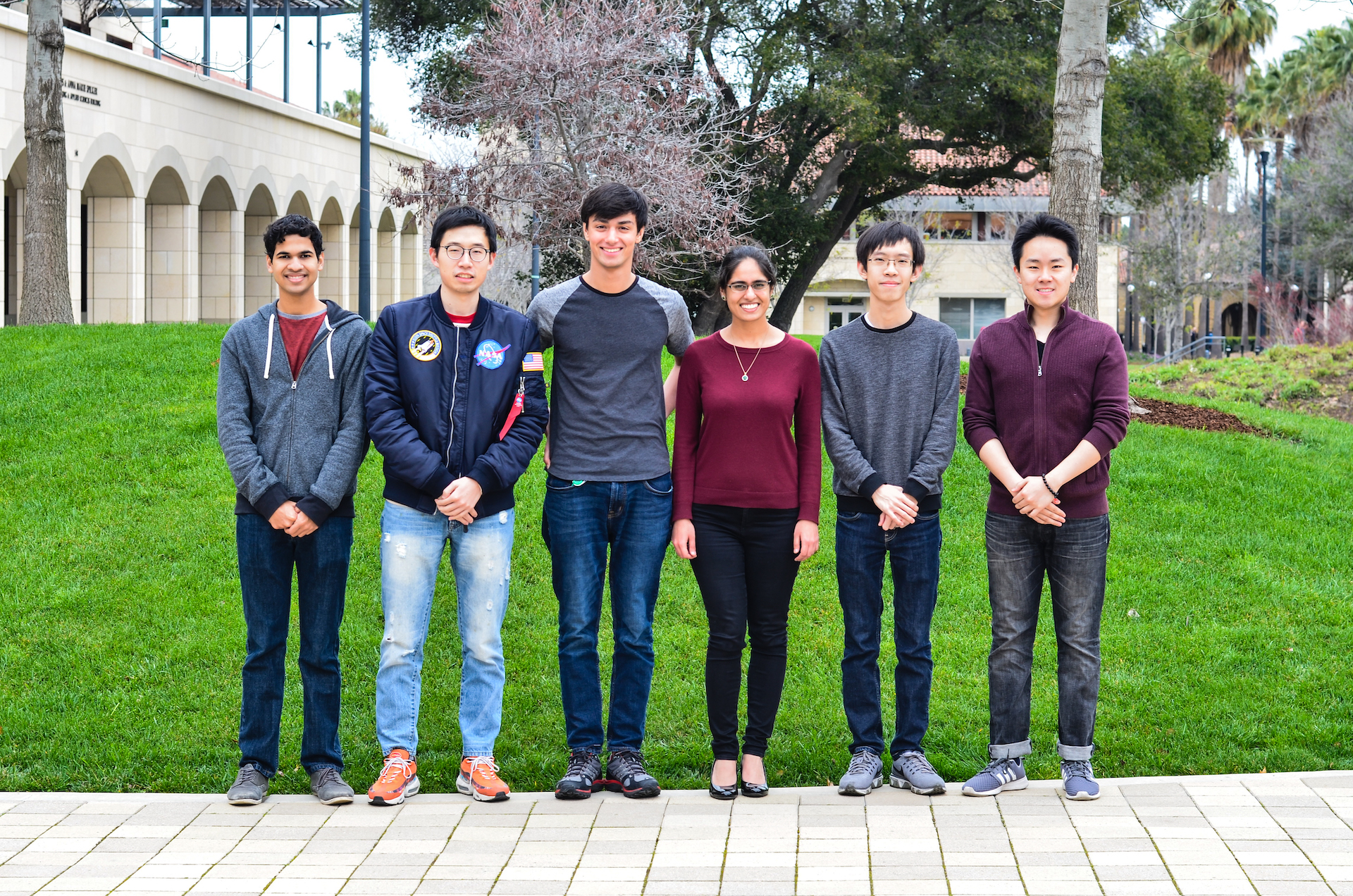
 Group photo from March 1, 2019. From left to right: Kartik Prabhu, Fei Huang, Akash Levy, Priyanka Raina, Haitong Li and Weier Wan.
Group photo from March 1, 2019. From left to right: Kartik Prabhu, Fei Huang, Akash Levy, Priyanka Raina, Haitong Li and Weier Wan.
Stanford accelerate group works in three areas:

| praina AT stanford DOT edu | |
|---|---|
| Contact | Allen Building - Room 114, (857) 209-8205 |
| About | Priyanka Raina is an Assistant Professor in Electrical Engineering at Stanford University. Previously, she was a Visiting Research Scientist in the Architecture Research Group at NVIDIA Corporation. She received her Ph.D. degree in 2018 and S.M. degree in 2013 in EECS from MIT and her B.Tech. degree in EE from IIT Delhi in 2011. |
| Teaching | Priyanka teaches EE271: Introduction to VLSI Systems in the Fall and EE272: Design Projects in VLSI Systems in the Winter. |

| klinej AT stanford DOT edu | |
|---|---|
| Contact | Packard Building - Room 359, (650) 723-4539 |
| About | Julie Kline is a Faculty Administrator at Stanford, and she supports several Electrical Engineering professors and their research teams. She holds a master’s degree in English from San Jose State University, and prior to her work at Stanford, she spent several years teaching academic writing and rhetoric at De Anza College in Cupertino. Julie is an active member at Coastal Repertory Theatre in Half Moon Bay, where in addition to acting, directing, and producing, she serves on several committees and the Board of Directors. |
| haitongl AT stanford DOT edu | |
|---|---|
| Webpage | https://web.stanford.edu/~haitongl |
| About | Haitong Li is an EE Ph.D. candidate at Stanford University, supervised by Prof. H.-S. Philip Wong and co-advised by Prof. Priyanka Raina. Previously, he was a Research Intern in the Device, Circuit and System (DCS) Group at Arm. He received M.S. in Electrical Engineering from Stanford University in 2017, and B.S. in Microelectronics from Peking University, China, in 2015. He is a recipient of 2016 IEEE EDS Masters Student Fellowship. |
| Research | My research is focused on in-memory computing enabled by emerging non-volatile memory technologies. The application space ranges from deep learning inference (DAC’19) to hyper-dimensional computing (IEDM’16, ISSCC’18) for cognitive applications, while leveraging the unique physical characteristics of emerging devices (e.g., stochasticity, 3D vertical connectivity). I also collaborate closely with Prof. Subhasish Mitra (Stanford) and Prof. Jan Rabaey (UC Berkeley). For more details, please refer to my Google Scholar profile. |

| weierwan AT stanford DOT edu | |
|---|---|
| Webpage | https://www.linkedin.com/in/weier-wan/ |
| About | Weier Wan is an EE Ph.D. candidate at Stanford University, supervised by Prof. H.-S. Philip Wong and co-advised by Prof. Priyanka Raina. Previously, he was a Research Intern at Google X. He received M.S. in Electrical Engineering from Stanford University in 2017, and B.S. in Electrical Enginnering and Computer Science and B.A. in Physics from UC Berkeley, in 2015. |
| Research | My research focuses on using resistive memory (RRAM) based analog in-memory computing to enable energy and area-efficient machine learning. Recently I designed and taped-out (and currently testing) a fully-integrated mixed-signal chip with RRAM synapses monolithically integrated with CMOS neurons. The chip implements inference and training for Restricted Boltzmann Machine, a type of probablistic graphical model, as well as inference for MLPs and RNNs. The project is a collaborative effort with Prof. Gert Cauwenberghs (UCSD) and Prof. Huaqiang Wu (Tsinghua University). I also studied novel techniques for quantizing deep neural networks (https://github.com/google-research/google-research/tree/master/cnn_quantization) |
| akashl AT stanford DOT edu | |
|---|---|
| Webpage | https://www.linkedin.com/in/akashlevy/ |
| About | Akash Levy is an EE Ph.D. student at Stanford University, supervised by Prof. Priyanka Raina. Previously, he was a Research Intern at Amazon Lab126 and Amazon Web Services. He received a B.S.E. degree in Electrical Engineering from Princeton University in 2018, with certificates in Applications of Computing and Engineering Physics. He is a recipient of the 2018 NSF Graduate Research Fellowship. |
| Research | My current research is focused on improving the efficiency of reconfigurable logic devices (such as FPGAs and CGRAs) through the use of 3D integration with emerging nanotechnologies. In particular, I am developing a hybrid design that makes use of both resistive random access memory (RRAM) and nanoelectromechanical (NEM) relays to implement reconfigurable switching in the back-end-of-line for reduced reconfigurability overhead. My ultimate goal is to enable reconfigurable logic devices to become more competitive with ASICs in terms of power, area, and performance. My pre-PhD research involved a broad range of subjects, ranging from physics to computer security. For more details, please refer to my Academia.edu portfolio and my Google Scholar profile. |

| kzf AT stanford DOT edu | |
|---|---|
| About | Kathleen Feng is an EE Ph.D. student at Stanford University, supervised by Prof. Priyanka Raina. She received a B.S.E. degree in Electrical Engineering from Princeton University in 2018, with certificates in Applications of Computing and Robotics and Intelligent Systems. She is a recipient of the NDSEG Fellowship. |
| Research | My current research focuses on accelerating deep image processing pipelines (ISPs) on reconfigurable hardware. Deep ISPs combine low-level image processing techniques with high-level image classification, allowing for a more robust process. More generally, I am interested in designing and developing new computer architectures for computer graphics, vision, and related applications. |
| kprabhu7 AT stanford DOT edu | |
|---|---|
| Webpage | https://linkedin.com/in/kprabhu7/ |
| About | Kartik Prabhu is an EE M.S. student at Stanford University. Previously, he was a software engineering intern at Cisco. He received a B.S. degree in Computer Engineering from Georgia Institute of Technology in 2018. |
| Research | My current research involves creating generators for DNN accelerators. The generator is written using high-level synthesis (HLS) to enable for the creation of a DNN accelerator given a set of parameters, and can generate many of the architectures that have been proposed. |

| mcoduoza AT stanford DOT edu | |
|---|---|
| Webpage | https://linkedin.com/in/michael-oduoza/ |
| About | Michael Oduoza is an EE co-term student at Stanford University. |
| Research | My current research is in the 3D integration of resistive random access memory (RRAM) and nanoelectromechanical (NEM) relays to create a hybrid CGRA design. This hybrid design has promise for reducing the reconfigurability overhead in programmable logic devices. |

| makenal AT stanford DOT edu | |
|---|---|
| Webpage | |
| About | Makena Low is an EE undergraduate student at Stanford University. |
| Research | My research is developing machine learning algorithms for dermatological image segmentation and area determination for diseases such as vitiligo and melanoma. |

| chtsao AT stanford DOT edu | |
|---|---|
| Webpage | https://www.linkedin.com/in/chtsao/ |
| About | Charles Tsao is an EE co-term student at Stanford University. |
| Research | My current research focuses on the SoC side of the AHA Project. I’m currently focused on building architecture and software API to support end-to-end hardware reconfiguration and execution on various hardware targets at the press of a button. This software API, called the Reconfigurable Device Access Interface (RDAI) API, layers over hardware accelerator API to allow a Halide application to run end-to-end on a custom hardware accelerator (e.g. FPGA, CGRA). |
People: Faculty - Priyanka Raina, Mark Horowitz, Pat Hanrahan, Clark Barrett, Kayvon Fatahalian, and many students advised by these faculty
The goals of the agile hardware project are
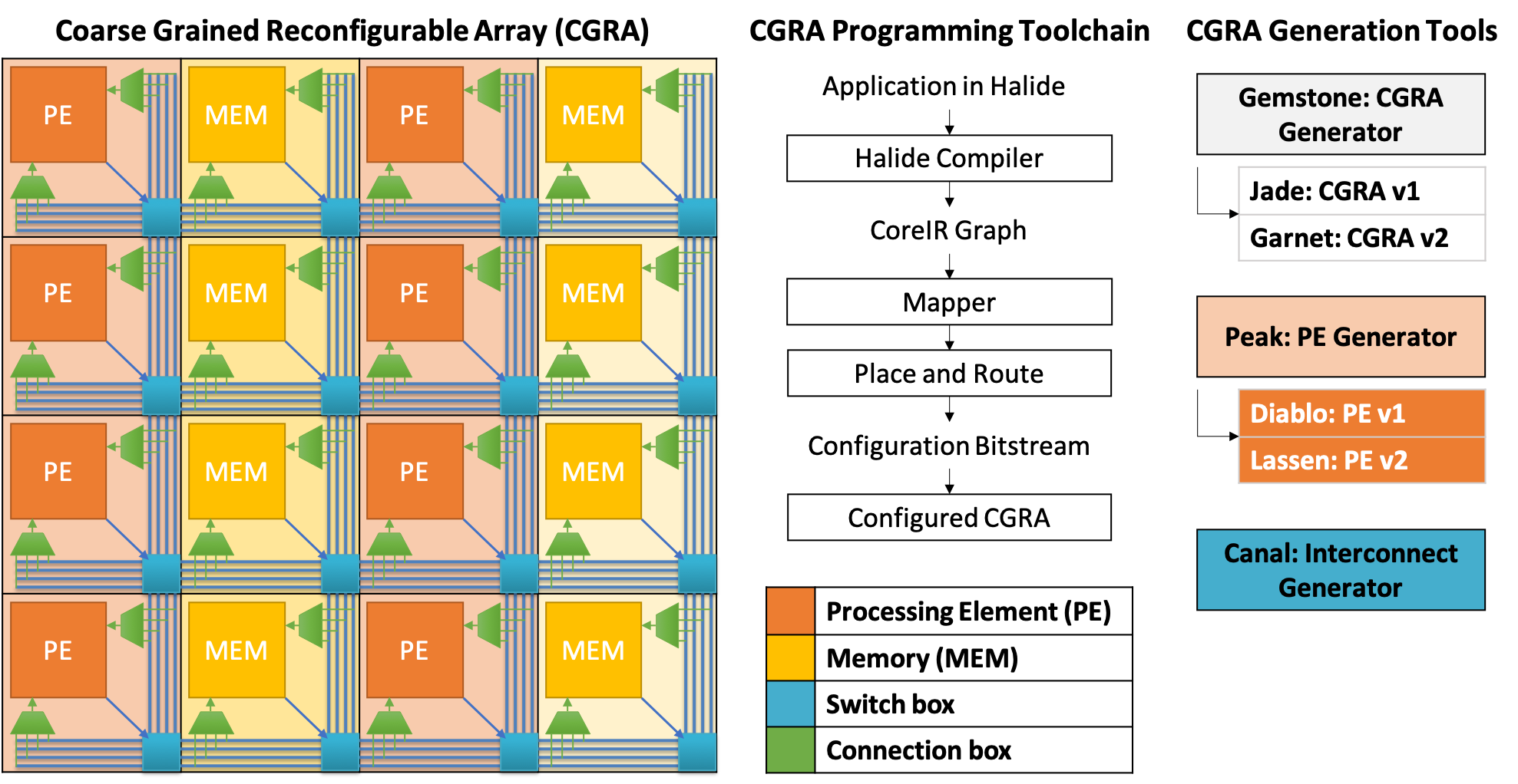
More information about the project can be found on the project webpage. All the hardware designed in the project and its programming toolchain are open-source and can be found on the project github. There are multiple faculty and students working on different parts of the project; described below are the parts that Priyanka is actively involved in:
Gemstone is a CGRA generation infrastructure that comprises
Garnet is our second generation CGRA. Compared to Jade, the first generation CGRA, garnet has several new features:
Code: Garnet
Peak is a domain specific language (DSL) embedded in python that we have designed to specify the processing element (PE) of our CGRA. The goal is to have the PE specification be the single source of truth, and have peak automatically generate RTL, testbench, mapper and documentation for the PE from it. Code: Peak
Lassen is our second generation PE. Compared to the first generation PE, Diablo, Lassen has several new features including support for BFloat add and multiply, and instructions that allow multiple PE and MEM tiles to be grouped to support transcendental functions such as div, log, e^x, sin and pow. Code: Lassen
In addition to the new CGRA, our next chip will have the first version of our SoC with a control processor and a flexible interconnect. We are invesitigating both ARM and RISC-V based designs.
People: Haitong Li, Philip Wong, Priyanka Raina
Machine and deep learning workloads have been moving from cloud to edge, due to real-time requirements, bandwidth challenges, and privacy concerns. Today’s edge computing solutions mainly provide inference capabilities. Yet, more complicated and realistic scnearios require ‘learning’ capabilities to meet the fast-changing environments at the user’s end. To realize this goal of delivering machine inteligence at edge, we plan to explore one-shot and few-shot learning, which essentially represent an online learning scenario with rapid acquisition of few unseen examples.
State-of-the-art memory-augmented neural networks (NNs) combine the best characteristics of parametric models (e.g., CNN/LSTM) and non-parametric models (e.g., nearest neighbors). The idea is that features extracted by front-end NNs can be stored in an associative memory, inspired by human’s working memory, where similarity measurement is the key to enabling rapid recall and reasoning for one/few-shot learning.
With the increasing complexity in feature space from multi-media data, hardware acceleration opportunities arise for efficient implementations of associative memories. Our approach is to explore in-memory computing architectures enabled by emerging non-volatile memory (NVM) technologies (e.g., resistive RAM). The unique capability is doing in-situ distance comparison in a non-volatile fashion. At the architecture level, we’re exploring the design spaces of the front-end feature extractor and the associative memories with realistic NVM characteristics, aimed at providing energy efficiency benefits for large-scale datasets.
People: Massimo Giordano, Rohan Doshi, Kartik Prabhu, Paul Chettupuzha Jolly, Robert M. Radway, Luke Upton, Binh Q. Le, Daniel Bankman, Subhasish Mitra, Boris Murmann, Priyanka Raina
The scale of deep neural networks (DNNs) trained on increasingly large datasets has rapidly outpaced the amount of memory that can be densely integrated on the same die as compute in conventional CMOS technology. This has created an energy and performance bottleneck at the interface with off-chip DRAM. With a theoretically 12F2 1T1R cell, multi-level capability, and the promise of monolithic 3D integration, resistive RAM (RRAM) offers a new, orthogonal path to significant strides in energy-efficiency and performance of DNN hardware. Driven bottom-up by this emerging technology, we propose a set of DNN hardware architectures which leverage the density of RRAM in both the near-memory, digital and in-memory, mixed-signal computing contexts.
People: Akash Levy, Michael Oduoza, Priyanka Raina


Field-programmable gate arrays (FPGAs) are programmable logic devices (PLDs) that enable rapid prototyping of digital circuits and provide an alternative to the expensive application-specific integrated circuit (ASIC) design process today. However, when compared with ASICs performing the same function, SRAM-based FPGAs typically have 10-40 times lower logic density, 3-4 times higher delay, and 5-12 times higher dynamic power dissipation. This is because reconfigurable components incur large overhead—instead of being packed tightly, configurable logic blocks (CLBs) in FPGAs are laid out relatively far apart to make space for routing components, resulting in greater interconnect delay, power dissipation, and chip area. The disparity in the performance of FPGAs and ASICs provides motivation to find ways to reduce reconfigurability overhead, so that ultimately PLDs can become competitive with ASICs at manufacturing scale. Possible solutions lie with PLD designs that trade off fine-grained CLBs with more specialized blocks e.g. coarse-grained reconfigurable arrays (CGRAs), or with emerging nanotechnologies that enable novel design strategies in the space of reconfigurable semiconductor devices (to be discussed later).
Another topic of interest in semiconductor design today is “normally off, instantly on” device operation, which is critical for devices with weak, unreliable, or intermittent power sources. Energy-harvesting devices, wearables, and low-power nodes in the Internet of Things (IoT) will need to be able to operate in this mode to prevent unnecessary power dissipation between periods of action. Today, FPGAs need to load their configuration from off-chip memory into SRAM on startup. This has motivated the development of integrated non-volatile memory (NVM) that can replace (or work well in conjunction with) on-chip SRAMs to enable intermittent computing.
In this project, we propose the use of two emerging nanotechnologies in PLD design for bridging the gap between PLDs and ASICs: resistive random access memory (RRAM) and nanoelectromechanical (NEM) relays. We describe a hybrid RRAM-NEM-based design for implementing PLDs with both “normally off, instantly on” device operation and low-overhead reconfigurable routing components. We exploit the properties of RRAM and NEM relays in a synergistic fashion to develop a novel NV-SRAM-based router that has all of its read circuitry implemented in back-end-of-line (BEOL), with RRAM cells directly controlling gate voltage of hysteretic NEM relays that behave as routers. We compare the design of a CGRA developed using the techniques described here versus designs that use (1) NEM relays only, (2) RRAM only, and (3) standard CMOS technologies (baseline).
People: Kartik Prabhu, Xuan Yang, Mark Horowitz, Priyanka Raina
Deep neural networks require custom accelerators in order to run with high performance and energy efficiency. Several DNN accelerators that have been proposed have very similar properties, with some form of a systolic array and a hierarchy of on-chip buffers. However, designing accelerators from scratch is very expensive in terms of time and resources. To get around this, we have created a generator framework using high-level synthesis that can create DNN accelerator designs with different parameters. In addition to this, we have a tool that performs design space exploration and finds the optimal set of parameters such as array and memory sizes in terms of energy and performance. The tool also finds the best scheduling (loop tiling and ordering) of any neural network layer on the accelerator. In other words, the system doesn’t just generate the accelerator hardware, but also the compiler for it. We are using this system as a class project in EE272, our chip design bootcamp class.
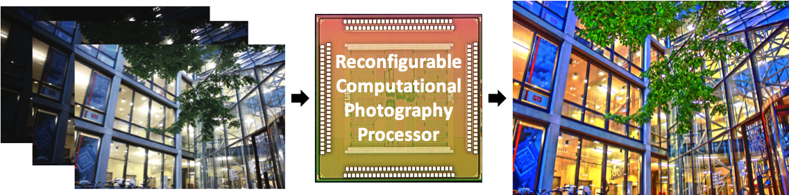
People: Kathleen Feng, Chris Metzler, Gordon Wetzstein, Priyanka Raina
The capacity of imaging systems must continue to expand in order to keep pace with rapidly increasing, application-specific demands in robotic and machine vision, consumer photography, autonomous driving, surveillance and machine learning. State-of-the-art imaging systems optimize the image processing pipeline (ISP) for image quality as perceived by a human observer and they treat different stages of the ISP as separate blocks, which leads to sub-optimal performance. In particular, sensor noise, defocus and motion blur, as well as other imperfections in the image formation, especially in low-light environments, are fundamental challenges for achieving state of the art performance of computer vision algorithms, such as image classification and object detection with current ISPs.
Stanford Computational Imaging Lab has proposed an optimization-based ISP approach that outperforms commercial implementations of Google Nexus phones significantly. They have recently explored novel end-to-end differentiable architecture for joint denoising, deblurring, and image classification that makes classification robust to realistic noise and blur. This architecture dramatically improves the accuracy of a classification network in low light and other challenging conditions, outperforming alternative approaches such as retraining the network on noisy and blurry images and preprocessing raw sensor inputs with conventional denoising and deblurring algorithms. The architecture learns denoising and deblurring pipelines optimized for classification whose outputs differ markedly from those of state-of-the-art denoising and deblurring methods, preserving fine detail at the cost of more noise and artifacts. These results suggest that the best low-level image processing for computer vision is different from existing algorithms designed to produce visually pleasing images.
At the same time, we recognize that the algorithms for computational imaging and vision are rapidly evolving, and hardware must follow suit: the next generation of hardware ISPs must be “programmable” to support new algorithms created with high-level frameworks. Our results for the AHA project suggest that the best programmable ISPs would be heterogeneous CGRAs with a multitude of small ASIC-style compute units.
In this project, we will design an end-to-end ISP pipeline for computer vision tasks, primarily focusing on the application of object detection. Moreover, we will explore deep neural network architectures that generalize across other applications, including segmentation, tracking, face detection, and more. A dedicated neural network will be trained for all of these applications separately, but the larger goal of this project is to develop a unifying network architecture that represents the state-of-the-art computer vision pipeline (optimizing high-level vision tasks). We will also create a CGRA hardware architecture (and its programming toolchain) with compute units optimized for running this unifying network at high performance and energy-efficiency. We expect the outcome of this project to lay the foundations of future energy-efficient and programmable mobile image processors.
People: Makena Low, Dr. Victor Huang (UC Davis), Priyanka Raina
Vitiligo is an autoimmune condition that targets melanocytes, the pigment producing cells of the skin, and results in large patches of skin losing their color. It affects approximately 1% of the population and has significant negative effects on the quality of life of patients. Vitiligo progresses over the course of months to years and response to treatment may, similarly, require months to years to become apparent. This is a significant hurdle as selecting an optimal treatment strategy such as immune suppression versus surgical approaches hinges on being able to accurately assess residual disease activity. However, there is no sensitive and objective outcome measure to characterize the spread of the disease, and this has been a major hurdle for optimizing clinical care as well as for development of clinical trials for vitiligo.
To assess the spread of vitiligo, a clinician commonly performs a visual examination of the patient and assigns a VASI (Vitiligo Area Scoring Index), or a VETF (Vitiligo European Task Force) score that corresponds to the depigmented body surface area (BSA) or ‘lesion(s)’. However, this method has low accuracy, high variability, and is insensitive to small changes. The gold standard of lesion area assessment involves planimetry, where a lesion is manually traced onto a transparent grid sheet from which area is calculated. This approach is time intensive, however, and limited to individual lesions and not suited to evaluating involvement across an entire body or region. There have been attempts at measuring relative change in lesion area using image analysis based on 2D color images which do not require manual lesion segmentation but they still introduce a 20-40% error in area calculated depending on the angle of image acquisition since the lesions are on curved body surfaces. Additionally, they only measure relative area change between two images taken at different times, and not absolute surface area.
We propose the development and clinical evaluation of a fully-automated computer-assisted system that quantitatively and accurately assesses 3D BSA using depth and color imaging and machine learning based vision algorithms. The greater sensitivity of this method will detect currently sub- clinical changes, which can be clinically significant in defining disease activity and predicting both initial response and durability of response to treatment. In addition, this technology can be later adapted for analysis of any skin condition for which BSA is an outcome measure of interest, such as psoriasis, melanoma, dermatological reactions to drugs and wounds.
People: Ali Hashemi, John Cioffi, Subhasish Mitra, Priyanka Raina
We are for students interested in working on this project. Please send Priyanka an email if you are interested.
People: Brucek Khailany, Rangharajan Venkatesan†, Yakun Sophia Shao, Brian Zimmer, Jason Clemons, Matthew Fojtik, Nan Jiang, Ben Keller, Alicia Klinefelter, Nathaniel Pinckney, Priyanka Raina, Stephen G. Tell, Yanqing Zhang, William J. Dally, Joel S. Emer, C. Thomas Gray, Stephen W. Keckler
In this work, a scalable deep neural network (DNN) inference accelerator consisting of 36 small chips connected in a mesh network on a multi-chip-module (MCM) was designed. The accelerator enables flexible scaling for efficient inference on a wide range of DNNs, from mobile to data center domains. The chip was implemented using a novel high-productivity VLSI methodology, fully designed in C++ using High-Level Synthesis (HLS) tools and leveraged an agile VLSI design flow. The 6 mm2 chip was implemented in 16nm technology and achieves 1.29 TOPS/mm2, 0.11 pJ/op energy effi- ciency, 4 TOPS peak performance on 1 chip, and 128 peak TOPS and 2,615 images/s ResNet-50 inference in a 36-chip MCM.
People: Angshuman Parashar, Priyanka Raina, Sophia Shao, Rangharajan Venkatesan, Yu-Hsin Chen, Brucek Khailany, Stephen W. Keckler, Joel Emer
Tensorloop is an infrastructure for evaluating and exploring the architecture design space of deep neural network (DNN) accelerators. Timeloop uses a concise and unified representation of the key architecture and implementation attributes of DNN accelerators to describe a broad space of hardware topologies. It can then emulate those topologies to generate an accurate projection of performance and energy efficiency for a DNN workload through a mapper that finds the best way to schedule operations and stage data on the specified architecture. This enables fair comparisons across different architectures and makes DNN accelerator design more systematic.
People: Priyanka Raina, Bill Freeman, Fredo Durand, Anantha Chandrakasan

People: Priyanka Raina, Mehul Tikekar, Bill Freeman, Fredo Durand, Anantha Chandrakasan

Camera shake is the leading cause of blur in cell-phone camera images. Removing blur requires deconvolving the blurred image with a kernel which is typically unknown and needs to be estimated from the blurred image. This kernel estimation is computationally intensive and takes several minutes on a CPU which makes it unsuitable for mobile devices.
This work presents the first hardware accelerator for kernel estimation for image deblurring applications. Our approach, using a multi-resolution IRLS deconvolution engine with DFT-based matrix multiplication, a high-throughput image correlator and a high-speed selective update based gradient projection solver, achieves a 78x reduction in kernel estimation runtime, and a 56x reduction in total deblurring time for a 1920 x 1080 image enabling quick feedback to the user. Configurability in kernel size and number of iterations gives up to 10x energy scalability, allowing the system to trade-off runtime with image quality. The test chip, fabricated in 40nm CMOS, consumes 105mJ for kernel estimation running at 83MHz and 0.9V, making it suitable for integration into mobile devices.
People: Rahul Rithe, Priyanka Raina, Nathan Ickes, S. V. Tenneti, Fredo Durand, Anantha Chandrakasan
Computational photography refers to a wide range of image capture and processing techniques that extend the capabilities of digital photography and allow users to take photographs that could not have been taken by a traditional camera. Since its inception less than a decade ago, the field today encompasses a wide range of techniques including high dynamic range (HDR) imaging, low light enhancement, panorama stitching, image deblurring and light field photography. These techniques have so far been software based, which leads to high energy consumption and typically no support for real-time processing.
This work focuses on a hardware accelerator for bilateral filtering which is commonly used in computational photography applications. Specifically, the 40 nm CMOS test chip performs HDR imaging, low light enhancement and glare reduction while operating from 98 MHz at 0.9 V to 25 MHz at 0.9 V. It processes 13 megapixels/s while consuming 17.8 mW at 98 MHz and 0.9 V, achieving significant energy reduction compared to previous CPU/GPU implementations, enabling real-time computational photography applications on mobile devices. Live demonstration at the ISSCC Demo Session. Video
People: Dongsuk Jeon, Nathan Ickes, Priyanka Raina, H. C. Wang, Anantha Chandrakasan
3D imaging devices, such as stereo and time-of-flight (ToF) cameras, measure distances to the observed points and generate a depth image where each pixel represents a distance to the corresponding location. The depth image can be converted into a 3D point cloud using simple linear operations. This spatial information provides detailed understanding of the environment and is currently employed in a wide range of applications such as human motion capture. However, its distinct characteristics from conventional color images necessitate different approaches to efficiently extract useful information.
This chip is a low-power vision processor for processing such 3D image data. The processor achieves high energy-efficiency through a parallelized reconfigurable architecture and hardware-oriented algorithmic optimizations. The processor will be used as a part of a navigation device for the visually impaired. This handheld or body-worn device is designed to detect safe areas and obstacles and provide feedback to a user. We employ a ToF camera as the main sensor in this system since it has a small form factor and requires relatively low computational complexity.
More details about Priyanka’s PhD work are on Priyanka’s MIT webpage.